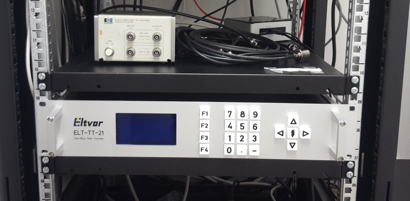
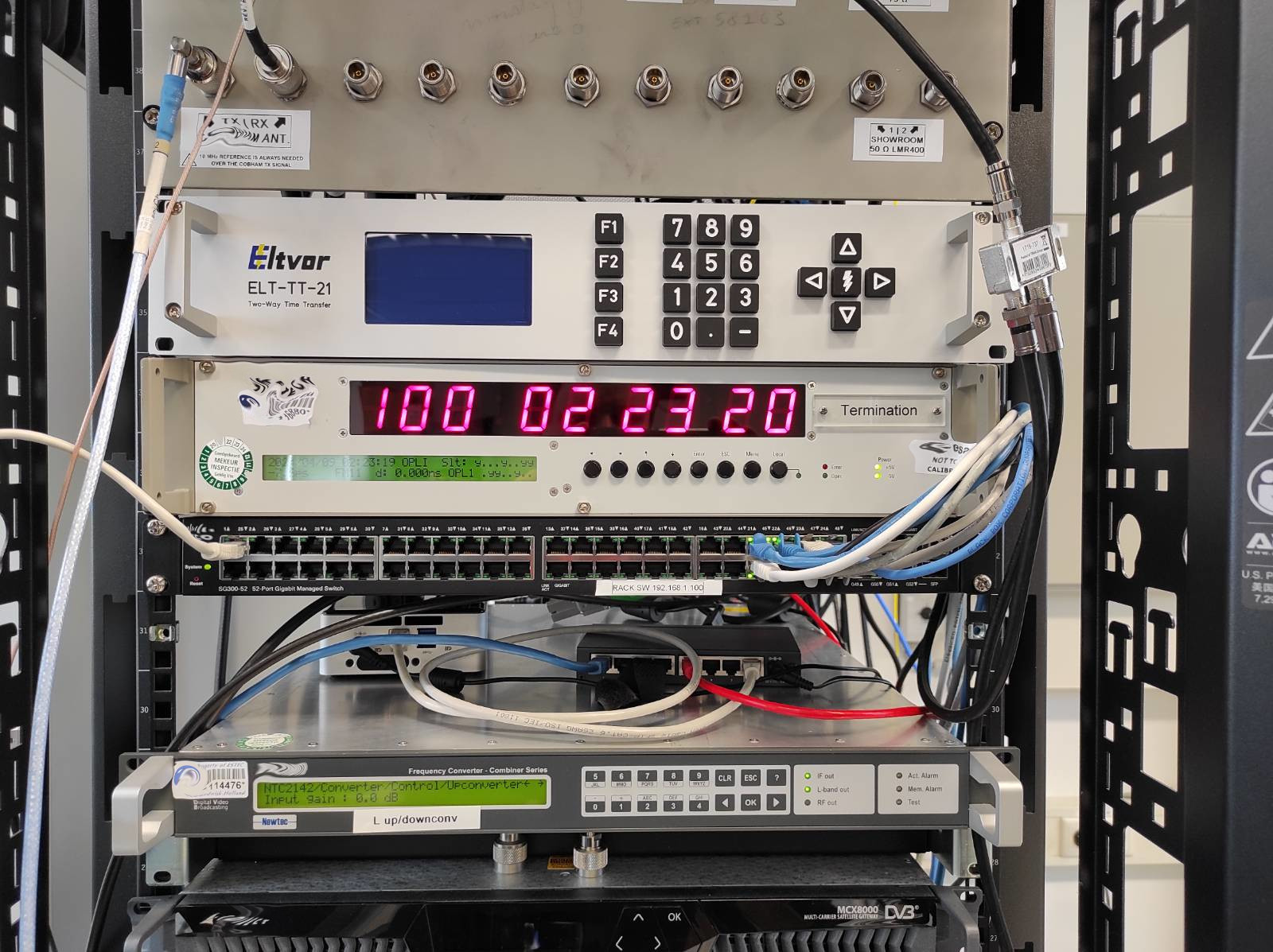
ELT-TT-21
-
Ground-station Two-Way Satellite Time and Frequency Transfer modem
-
1 Tx and 8 Rx CDMA channels
-
Low systematic errors by design, fully digital implementation
-
Fully compatible with current BIMP/UTC TWSTFT modulation and codes
-
Manual as well as remote configuration/commanding
-
Code phase jitter (Tx → Rx1 loopback), duration 600s, τ = 1s:
chiprate σ(τ = 1s)[ps RMS ] 1M 1.8 2.5M 0.5 5M 0.3 10M 0.1 20M 0.1
The Two-Way Satellite Time and Frequency Transfer (TWSTFT) modem is designed to allow highly accurate transfer and/or comparison of time among two or more ground stations via a satellite bent-pipe transponder. The general principle complies with [ITU]. Two or more ground stations are connected to shared satellite channel. All these stations do have some local realisation of the time to be compared to the others. Two-way ranging measurements between any of the two stations are disseminated in a standardised data file format.
Each modem generates a PN-spread ranging signal, which is being transmitted to the satellite. At the same time, the modem receives from the satellite the transponded and delayed echo of own signal, plus superimposed signals from all other stations. In real time, the receiver section processes the received signal and estimates the code delay and carrier phase which are the outputs of the modem.
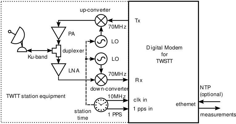
The target electrical specification for the interfaces are summarised in Table 1.
Table 1. Electrical interface description
| I/F | Parameter | Specification | Condition / note |
|---|---|---|---|
| Tx | frequency range | 0…100 MHz | nominally 70±20 MHz |
| output level | −50…+3 dBm | ||
| impedance | 50 Ω | ||
| reflection coefficient | −15 dB | ||
| Tx mon | output level other | −60…−7 dBm | fixed Tx −10 dB |
| other | same as Tx | ||
| Rx1, Rx2 | frequency range | 0…100 MHz | nominally 70±20 MHz |
| input level | −50…+3 dBm | ||
| impedance | 50 Ω | ||
| reflection coefficient | −15 dB | ||
| Clk in | frequency | 10 MHz | |
| input level | −10…+10 dBm | ||
| impedance | 50 Ω | ||
| reflection coefficient | −15 dB | ||
| 1 pps in | input level | 0…5 V | |
| impedance | 10kΩ | ||
| Clk out | frequency | 10 MHz | |
| output level | 10 dBm | ||
| impedance | 50 Ω | ||
| reflection coefficient | −15 dB | ||
| 1 pps out | output level | 0/4 V | |
| impedance | 50 Ω |
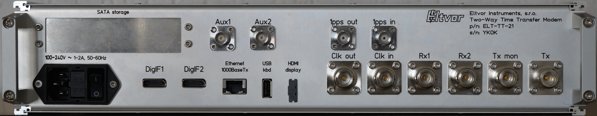
The modem is housed in a 2U 19 inch rack chassis. The external interfaces of the modem for both front and rear panels are listed in tables below. The modem baseline is 70 MHz intermediate frequency only.
Table 2. Modem rear panel interface description
| Interface | Physical | Description |
|---|---|---|
| Rear panel | ||
| Tx | N | Tx Intermediate frequency (70 MHz) |
| Tx monitor | N | Tx, −10 dB |
| Rx1, Rx2 | N | Rx Intermediate frequency (70 MHz) |
| Clock in | N | 10 MHz reference clock input |
| 1 pps in | BNC | 1-second frame signal complementing Clock in |
| Clock out | N | 10 MHz synthesized clock output |
| 1 pps out | BNC | 1-second frame signal complementing Clock out |
| Ethernet | 1000Base-Tx (RJ45) | NTP, measurement and control |
| 2x Monitor | BNC, LVCMOS | Generic digital monitoring/debug signals |
| Keyboard | USB-A | User external keyboard input |
| External display | HDMI | Output for external display for extended information about modem operational status |
| SSD storage | 2.5" SATA | Removable drawer for SATA SSD (bit-grabber, high-speed logging) |
| 2x digital data interface | Display port | Digital data interface for future use, e.g., for transfer of sampled data between cascaded modems |
| Power supply | IEC C14 | 100V–240V power supply input |
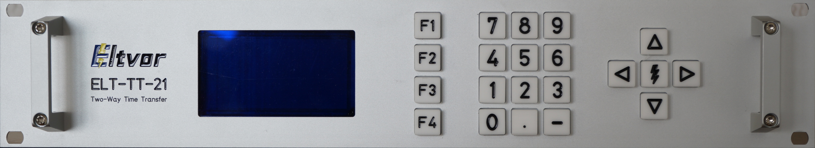
Table 3. Modem front panel interface description
| Interface | Physical | Description |
|---|---|---|
| Front panel | ||
| Display | VFD | User interface |
| Keypad | built-in pushbuttons | User interface (subset of essential functions) |
-
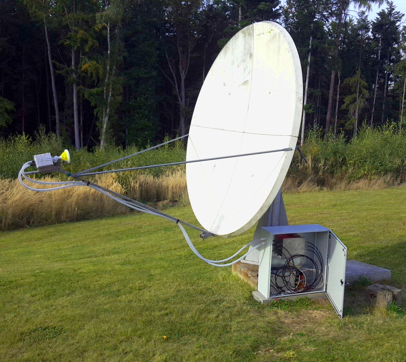
G/S: Pecný, 2.4m Ku-band terminal equipped with Eltvor RF signal path
-
antenna, ground works, cabling – all done/procured by Eltvor; passive (Rx-only) mode running for 2 years
-
-
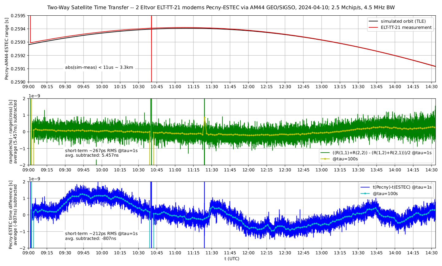
S/C: Express AM-44 (11W); (SIGSO - Slightly Inclined Geo-Synchronous Orbit – a retired GEO sat)
-
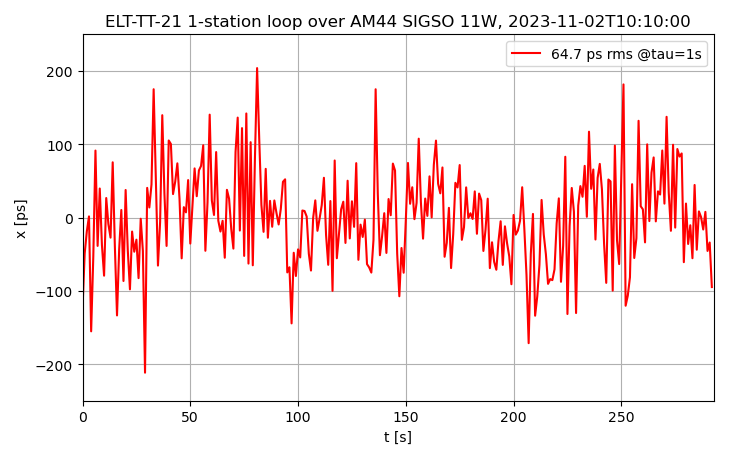
2.5Mchip/s, duration 300s, 4.5MHz BW → σ(τ = 1s) = 64.7ps RMS
-
Pecný ↔ AM-44 ↔ ESTEC, 780 km baseline
-
ELT-TT-21 installed at both sites
-
Results:
-
Legend:
-
Pecný–AM-44–ESTEC range [s]: measured delay vs. TLE-calculated
-
difference between 2 range measurements:
-
L1 = 1/2[echo(Pecný) + echo(ESTEC)]
-
L2 = 1/2[delay(Pecný,ESTEC) + delay(ESTEC,Pecný)]
-
-
UTC(Pecný)-UTC(ESTEC): measured TWSTFT vs. assumed equal
-
-
Comments:
-
ideal vacuum assumed, no iono, no Sagnac corrections
-
2 glitches due to transponder interference
-
1st glitch: ESTEC operator shut down Tx, Rx'es re-locked
-
2nd glitch: Tx remained on – Rx'es locked, increased jitter RMS
-
... both gracefully recovered
-
-
due to SIGSO:
-
90km pk-pk range drift, apogee, both high&low Doppler, amplitude fading
-
-
time difference vs. GNSS-referenced UTC: ±1ns
-
reference time diff between UTC(ESTEC) & UTC(TP) itself varying ≈ ±1ns
-
-
The FPGA firmware as well as SW is flexible enough to support various types of modulations and modulation parameters. Notably: independent PN-code on I/Q carriers (“QPSK mode”), data-less pilot signal, SinBOC/CosBOS subcarriers. E.g. a broad range of existing GNSS signals may be received and/or transmitted.
Nevertheless Eltvor sees a great opportunity in such a configurability: apart from optimising the TWSTFT performance, it may be useful to receive e.g. GNSS or other DSSS signals using the same modem as TWSTFT signals in order to support various inter-system calibrations.